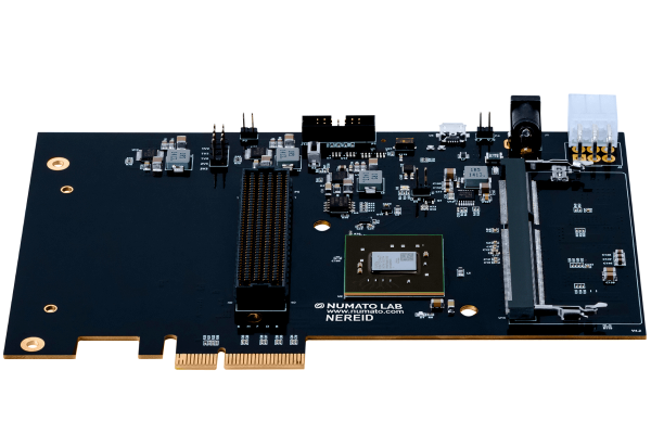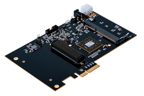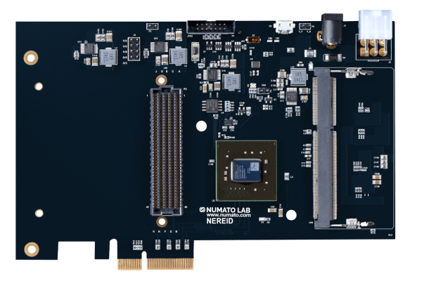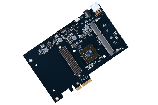


Nereid is an easy to use FPGA Development Board featuring Xilinx Kintex-7 FPGA with x4 PCIe interface and 4GB DDR3 SDRAM. This board features Xilinx XC7K160T– FBG676 FPGA. Other FPGA configurations are available at request.
Applications
| Title | Date | Download |
|---|---|---|
| User Manual | Feb 13 2018 | Download |
| Download Nereid XDC Constraints For Vivado | Feb 13 2018 | Download |
| Nereid BSP for Vivado | Feb 13 2018 | Download |
| Aug 02 2018 | Download | |
| Jul 01 2020 | Download | |
| Dec 01 2020 | Download | |
| Apr 01 2021 | Download | |
| Oct 22 2021 | Download | |
| Jan 21 2022 | Download | |
| Oct 07 2022 | Download | |
| Oct 07 2022 | Download | |
| Oct 07 2022 | Download | |
| Nov 10 2022 | Download | |
| Dec 09 2023 | Download | |
| Dec 09 2023 | Download |
Nereid is an easy to use FPGA Development Board featuring Xilinx Kintex-7 FPGA with x4 PCIe interface and 4GB DDR3 SDRAM. This board features Xilinx XC7K160T– FBG676 FPGA. Other FPGA configurations are available at request. The board features High Pin Count (HPC) high speed FMC connector for the purpose of adding additional features to the board by using custom or commercial-off-the-shelf daughter boards.

Features
Applications
| Weight | 1.50 lbs |
|---|---|
| Dimensions | 15.00 x 14.00 x 3.00 in |
| FPGA | |
| Memory | |
| Number Of Clock Sources |
3 |
| Communication |
x4 PCIe, USB-RS232 |
| Configuration Options |
JTAG |
| Primary Clock Frequency | |
| Number Of GPIOs (Max) |
153 |
| Non-Volatile Configuration Storage |
N25Q128A13ESE40E |
| Total Number of GTX |
4 |
| Differential Pairs Length Matched |
Yes |
| Language/Technology | IDE/Compiler | Type | OS | Download |
|---|---|---|---|---|
| Download |
| Name | Part# | Type |
|---|---|---|
| DC Power Line Communication (PLC) Reference Design | 24VDCPLCEVM | Evaluation Modules & Boards |
| Three Phase BLDC & PMSM Motor Kit with DRV8301 and Piccolo MCU | DRV8301-HC-C2-KIT | Evaluation Modules & Boards |