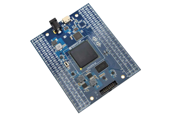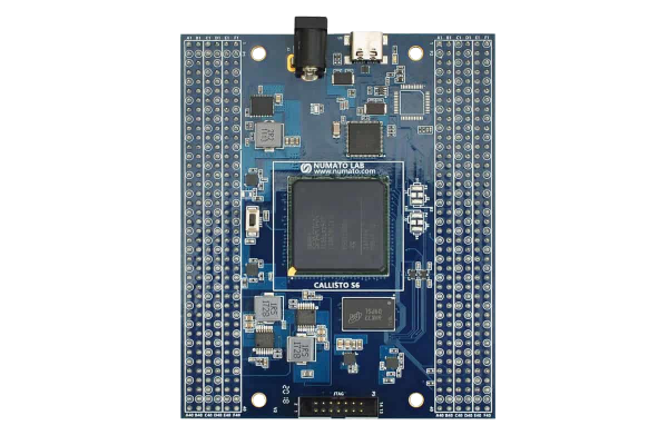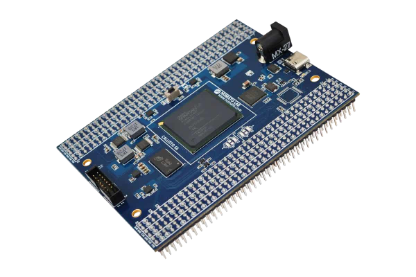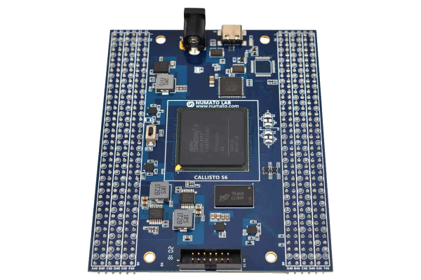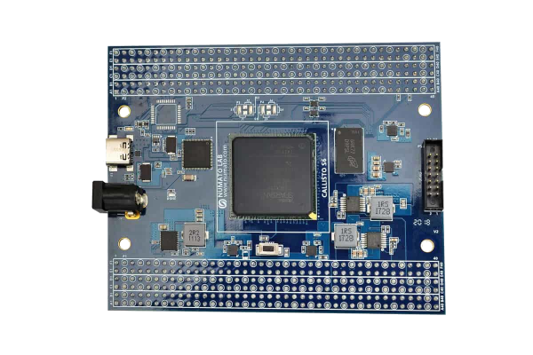
Callisto Spartan 6 is an easy to use FPGA Development board featuring the Xilinx Spartan 6 FPGA with 2Gb DDR3 SDRAM. This board contains the Xilinx XC6SLX150– FGG676 FPGA. The high-speed USB 3.1 interface (USB-C connector) provides fast and easy configuration download to the onboard SPI flash. There is no need for a programmer or special downloader cable to download bitstream to the board. The Development board also provides easy access to JTAG signals on a standard Xilinx Platform Cable compatible header. Callisto S6 provides the user the flexibility of adding their own peripherals through IO Expansion Headers.
Features
| Title | Date | Download |
|---|---|---|
| User Manual | Apr 14 2019 | Download |
| Apr 14 2019 | Download | |
| Oct 22 2021 | Download | |
| Jan 21 2022 | Download | |
| Nov 10 2022 | Download |
Callisto S6 is an easy to use FPGA Development board featuring the Xilinx Spartan 6 FPGA with 2Gb DDR3 SDRAM. This board contains the Xilinx XC6SLX150– FGG676 FPGA. The high-speed USB 3.1 interface (USB-C connector) provides fast and easy configuration download to the onboard SPI flash. There is no need for a programmer or special downloader cable to download bitstream to the board. The Development board also provides easy access to JTAG signals on a standard Xilinx Platform Cable compatible header. Callisto S6 provides the user the flexibility of adding their own peripherals through IO Expansion Headers.
Features
Applications
| FPGA | |
|---|---|
| Memory | |
| Number Of GPIOs (Max) |
284 |
| Configuration Options |
JTAG |
| Non-Volatile Configuration Storage |
N25Q128A13ESE40E |
| Number of Clock Sources |
2 |
| Communication |
USB 3.1 |
| Primary Clock Frequency |
| Language/Technology | IDE/Compiler | Type | OS | Download |
|---|---|---|---|---|
| Download |
| Name | Part# | Type |
|---|---|---|
| DC Power Line Communication (PLC) Reference Design | 24VDCPLCEVM | Evaluation Modules & Boards |
| Three Phase BLDC & PMSM Motor Kit with DRV8301 and Piccolo MCU | DRV8301-HC-C2-KIT | Evaluation Modules & Boards |